Fifofum: FIFO generator
© Copyright 2007 Adrian Lewis
 

Features
Download
Why
FIFOs
Sync-FF
Dual-port
Single-port
Async-FF
Low-power
Timing
Running
GUI
Make


Fifofum Home Page

Fifofum is a GUI-based tool for building FIFOs in Verilog HDL. Fifofum can generate FIFOs that store entries in either flip-flops, single-port memories, or dual-port memories. All FIFOs use a standard interface and protocol regardless of the storage type. Fifofum can also generate asynchronous FIFOs for sending data between two clock domains.

Features

  • Fifofum provides an easy-to-use GUI but can also be integrated into an automatic build environment.
  • Fifofum can generate a testbench and test your FIFO configuration.
  • Builds synchronous FIFOs based on flip-flops, single or dual port memories.
  • Builds asynchronous FIFOs based on flip-flops.
  • FIFOs use a standard interface regardless of storage implementation.
  • Optional outputs: full, empty, count, and space.
  • Optional inputs: per-clock-domain synchronous reset for asynchronous FIFOs.
  • Low-power option gates clock to all flop-based entries except the one being written.
  • Open source: standard GNU License, no sign-up required, no special conditions of use!

Download

Fifofum is included in the Prepro release.

Why use Fifofum?

Most ASIC design groups develop a library of modules that perform common and useful tasks; FIFOs and arbiters are obvious examples. This approach is much more efficient than having each designer create and test their own implementation. However, there are lots of possible FIFO types and options, and building a design library is not the primary goal of an ASIC development group. Fifofum can generate lots of different FIFO configurations with plenty of options, so why develop your own library?

The choice of storage medium for FIFO entries depends on the FIFO size and access requirements. For FIFOs containing less than 1k bits, a flip-flop implementation is usually more efficient than a memory-based implementation; using a single-port memory rather than a dual-port memory saves area but halves the bandwidth available for data transfers. As design constraints often change during or after the initial design phase, having a consistant interface regardless of storage type is highly desirable; the FIFO size and type can be changed without having to change the logic that interfaces to the FIFO. Fifofum generates FIFOs that use a standard interface, which makes migrating between storage implementations transparent to the surrounding logic, aside from changes in timing characteristics.

Fifofum FIFOs also support lots of cool features - quite literally in the case of the low-power option. There are also lots of optional extras, but as the FIFOs are fully configurable, you only get the options you need.

FIFO specifications

Standard Interface

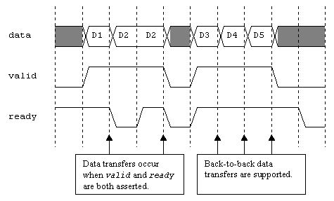
Both the read and write interfaces to Fifofum FIFOs are based on the same standard interface using the same protocol. The source data bus is qualified with a valid signal. The receiver asserts a ready signal when it is prepared to accept valid data. At the end of each clock cycle, data is transferred if both the valid and ready signals are asserted.

An important characteristic of this protocol is that FIFOs using this protocol may be connected in series without any additional glue logic. User logic using this protocol may also be connected in series to FIFOs or other similar logic.

Optional outputs

Regardless of FIFO type, a FIFO may be configured to include four optional outputs: wr_full, wr_space, rd_empty, rd_count; which indicate the current state of the FIFO.
  • wr_full is asserted if there are no unused FIFO entries.
  • wr_space is the number of unused FIFO entries.
  • rd_empty is asserted if there are no FIFO entries storing valid data.
  • rd_count is the number of FIFO entries storing valid data.
Please note that these outputs should never be used to replace the data-valid-ready interface; it is not always true that wr_full is the inverse of wr_ready, neither is it always true that rd_empty is the inverse of rd_valid.

Synchronous flip-flop based FIFOs

Fifofum generates flip-flop based FIFOs of any bit width and any depth. In general it is not possible to write to the FIFO when it is full, even if the FIFO is being read on the same cycle. For one-entry-deep FIFOs, it is possible to write when the FIFO is full provided that the FIFO is also being read; note that this feature creates a timing path between rd_ready and wr_ready.

FIFO entries are stored in arrays of flip-flops, either a simple Verilog memory or, in the low power configuration, an array of flop-flops per-FIFO-entry. Details of the low-power implementation are documented below.

Synchronous dual-port memory-based FIFOs

Fifofum generates dual-port memory-based FIFOs of any bit width and any depth. For mid-sized FIFOs, a FIFO based on a dual-port memory is more area efficient than a FIFO based on flip-flips, though it is important to take into account routing area to the memory and memory-BIST logic.

These FIFOs provide two additional interfaces for connection to the read and write ports of a user-provided dual-port memory. The write port interface contains three signals:

  • wp_address is the address of the entry being written.
  • When wp_write is asserted, data is written to the memory at the address provided.
  • wp_data is the data being written to the memory.
The read port interface contains three signals:
  • rp_address is the address of the entry being read.
  • When rp_read is asserted, data is read from the memory at the address provided.
  • On the clock cycle after rp_read is asserted, rp_data is the data read from the memory.

Synchronous single-port memory-based FIFOs

Fifofum generates single-port memory-based FIFOs of any bit width and any depth. For large FIFOs, a FIFO based on a single-port memory is more area efficient than a FIFO based on a dual-port memory, though it is important to understand the performance implications of this implementation. For FIFOs based on flip-flops and dual-port memories, it is possible to read and write simultaneously and continuously for as long as the user requires. FIFOs based on single-port memories have half the memory bandwidth of FIFOs base on a dual-port memory; simultaneous reads and writes are not possible. If both operations are requested on the same cycle, priority can either be given to the read or the write operation. Fifofum can generate single-port FIFOs with either read or write priority. Note that if the FIFO is configured with read-priority, a timing path exists between rd_ready and wr_ready.

These FIFOs provide an additional interface for connection to a user-provided single-port memory. The interface contains five signals:

  • sp_address is the address of the entry being accessed.
  • When sp_access is asserted, data is either read from or written to the memory at the address provided.
  • When both wp_write and sp_access are asserted, data is written to the memory at the address provided.
  • wp_data is the data being written to the memory.
  • On the clock cycle after sp_access is asserted and wp_write is de-asserted, rp_data is the data read from the memory.

Asynchronous flip-flop based FIFOs

Fifofum generates asynchronous flip-flop-based FIFOs of any bit width. The depth of the asynchronous FIFOs must be 2 to the power of any positive, non-zero, integer, i.e. 2, 4, 8, etc. The read and write interfaces of these FIFOs can operate on two independent clock domains. All wr_* signals are synchronous to wr_clock; all rd_* signals are synchronous to rd_clock. There are no restrictions on the either clock frequency other than normal intra-domain timing constraints.

Both clock domains have their own asynchronous reset input (wr_reset_n and rd_reset_n) and should both be asserted during chip reset. However if your application requires support for reseting one rather than both clock domains, then asserting a single asynchronous reset may have an undesireable side-effect. If only one asynchronous reset is asserted, then an empty FIFO might appear to contain data after reset is de-asserted. Optional synchronous resets (wr_reset and rd_reset) allow reset in one domain to reset the FIFO pointer logic in both domains, and hence an empty FIFO will remain empty before and after reset.

The asynchronous FIFO maintains two gray-code counters, one in each domain. As both interfaces use the value of both counters, the value of each counter is double-synchronized for use by the other clock domain. The use of gray code ensures that the value captured by the receiving clock domain is either the current or next counter value as the value changes. The synchronous reset must also be passed to both domains to ensure that both counter are reset and that an empty FIFO remains empty throughout the reset operation. A double-synchronizer is used to avoid meta-stablity in the receiving clock domain.

FIFO entries are stored in arrays of flip-flops, either a simple Verilog memory or, in the low power configuration, an array of flop-flops per-FIFO-entry. Details of the low-power implementation are documented below.

Low-power clock gating

FIFO entries are stored in arrays of flip-flops, either a simple Verilog memory or, in the low power configuration, an array of flop-flops per-FIFO-entry. In the low-power configuration, the array of flip-flops for each entry has a gated clock which is only enabled when that entry is being written.

Low-power FIFOs have a scan_mode input; it is used to enable the gated-clock when scan testing is in progress.

The user can either provide the name of the clock-gate module or use the clock-gate module (fff_gate) provided by Fifofum. The user supplied module must support the inputs, outputs, and functionality of the Fifofum clock gate module, though the internal implementation is user defined.

  • Inputs: in - the ungated clock; enable - the clock enable signal.
  • Output: out - the gated clock.
  • Functionality: out = in when enable is asserted, otherwise out holds its value regardless of the value of in.

Timing characteristics

General FIFO interface signals and timing
reset_n wr_reset_n rd_reset_n Asynchronous active-low reset.
wr_data For FIFOs based on flip-flops each bit of this bus has a fanout equal to the depth of the FIFO, but no logic before the flops. For FIFOs based on a memory, this bus drives the data input of the memory.
wr_valid This signal effects the state of most control registers in the FIFO and writes to the FIFOs entry storage. It also controls outputs to FIFO memory: sp_address, sp_access and wp_write.
wr_ready Output of a flip-flop except in the case of a FIFO based on a single-port memory configured with read-priority; a timing path exists between rd_ready and wr_ready.
wr_full Output of a flip-flop.
wr_space Output of flip-flops.
rd_data For FIFOs based on flip-flops the data is the multiplexed output of the entry storage flip-flops. For FIFOs based on a memory, this bus is driven directly from the data output of the memory.
rd_valid Output of a flip-flop.
rd_ready This signal effects the state of most control registers in the FIFO. It also controls outputs to FIFO memory: sp_address, sp_access, rp_address, rp_read, and, for single-port read-priority configuration, wp_write.
rd_empty Output of a flip-flop.
rd_count Output of flip-flops.
Dual-port FIFO memory interface signals and timing
wp_address Output of flip-flops.
wp_write Memory write is asserted as a combinatorial function of the control state of the FIFO and the wr_valid input.
wp_data The write-data input of the FIFO (wr_data) is passed directly to the input of the memory.
rp_address The read address of the memory access is either the read pointer, or the read pointer plus one - both registered values. The selection is a combinatorial function of the control state of the FIFO and the rd_ready input.
rp_read Memory read is asserted as a combinatorial function of the control state of the FIFO and the rd_ready input.
rp_data The read-data output of the memory is passed directly to the read-data output of the FIFO (rd_data).
Single-port FIFO memory interface signals and timing
sp_address The address of the memory access is either the write pointer, the read pointer, or the read pointer plus one - all registered values. The selection is a combinatorial function of the control state of the FIFO and the wr_valid and rd_ready inputs.
sp_access Memory access is asserted as a combinatorial function of the control state of the FIFO and the wr_valid and rd_ready inputs.
wp_write Memory write is asserted as a combinatorial function of the control state of the FIFO and the wr_valid input and, in the case of the read-priority configuration, the rd_ready input.
wp_data The write-data input of the FIFO (wr_data) is passed directly to the input of the memory.
rp_data The output of the memory is passed directly to the read-data output of the FIFO (rd_data).

Building FIFOs with Fifofum

Fifofum is a Python/Tk script. There are no arguments, just type fifofum to invoke the script and start the GUI. Once the desired FIFO configuration has been specified, the FIFO and an option test-bench can be built. Fifofum generates a makefile <module>.make, then runs make using the generated makefile. Make will build <module>.v and, optionally, the testbench fff_test.v.

Building FIFOs using the GUI

The GUI is divided into five vertically-stacked sections:

  1. Name, dimensions, and interface
    • Module: the name of the verilog module implementing the FIFO.
    • Depth: the depth of the FIFO, i.e. the maximum number of entries that can be stored.
    • Width: the width of each FIFO entry in bits.
    • Outputs: include optional FIFO status outputs.
      • Full: wr_full is asserted if there are no unused FIFO entries.
      • Space: wr_space is the number of unused FIFO entries.
      • Empty: rd_empty is asserted if there are no FIFO entries storing valid data.
      • Count: rd_count is the number of FIFO entries storing valid data.
    • Sync-reset: Synchronous resets wr_reset and rd_reset allow reset in one domain to reset the FIFO pointer logic in both domains. This logic allows reset to be asserted from only one clock domain.
  2. Storage and internal configuration
    • Flip-flops: select storage based on flip-flops. Options select between synchronous and asynchronous FIFO types; normal or low-power operation. The name of an externally defined clock gate can be specified, otherwise the fff_gate module will be defined and instantiated.
    • Dual-port: select storage based on a dual-port memory.
    • Single-port: select storage based on a single-port memory. The FIFO must be configured for either read-priority or write-priority as this determines which operation occurs when both operations are valid.
  3. Build and test options
    • Build options: Build the FIFO; or build the FIFO and testbench; or build the FIFO and testbench and run the simulation using the Icarus Verilog simulator.
    • Sim cycles: The number of clock cycles used when testing the FIFO in simulation.
  4. Actions
    • Build: Build the FIFO according to the specification. Build and run the testbench depending on the build options.
    • Clean: Delete generated files for the specified FIFO.
    • Reset: Reset the FIFO configuration to the initial blank settings.
    • Quit: Quit using Fifofum.
  5. Status
    • Black: display the current FIFO specification.
    • Red: describe an error in the FIFO specification.

Building FIFOs using Make

GUIs are not for everyone and it is often preferable to build on-the-fly rather than save generated source code. If you're building your source code tree using make, then building FIFOs with Fifofum couldn't be easier. Fifofum generates a Makefile for each FIFO built using the GUI. You can build FIFOs using your Makefile by integrating build rules extracted from the makefiles generated by Fifofum.

For example, the following rule can be extracted from the example.make, where example is a low-power, synchronous, 32-by-8, flip-flop-based FIFO, with the optional rd_empty output:

example.v: fff_fifo.plv example.make
  prepro -r '#$$' -r '<#;>' -r '>#;>' -r '#[;]#' -o $@ $< ++ example:fflp32x8e +fff_gate
Where fff_fifo.plv is the Prepro source for all Fifofum FIFOs; example:fflp32x8e is a condensed description of the FIFO specification; and +fff_gate specifies name of the external clock gate module.

This website uses CSS stylesheets and Frames.